How are Billions of Nanoscopic Transistors Made into a Microchip? EUV Photolithography 🛠️⚙️🤯


How are Billions of Nanoscopic Transistors Made into a Microchip? EUV Photolithography 🛠️⚙️🤯 with tags chip manufacturing, extreme ultraviolet, semiconductor industry, high na, high na euv lithography, microchips, microchip manufacturing, semiconductor manufacturing, euv, chip production, cpu, gpu, soc, ssds, semiconductor manufacturing, asml, tsmc, applied materials, semiconductor, fab, fabrication, how chips are made?, how semiconductors are made, chips explained, microchips explained, microchip printer, asml tool, duv, asml machine, apple, silicon wafer, computer chips, asml company
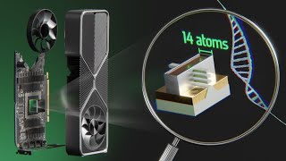
Inside microchips are nanometer-sized transistors and wires, but how are these nanoscopic structures built? Well, in this video, we’ll explore the EUV Photolithography System built by ASML. This 150-million-dollar machine is essentially a microchip photocopier; it takes the design of a microchip and copies it across hundreds of microchips on a silicon wafer. This EUV Photolithography System is one of the most complex machines ever made, and it encompasses an entire world of science and engineering within it. Specifically in this video, we'll dive deep into the EUV Lithography tool and explore how 13nm EUV light is produced, how the EUV light is focused onto a photomask, how the photomask, or mask, moves around, what the patterns on the mask look like, the projection optics, and how the wafer moves around and the wafer stage. So join us on this adventure into the world of EUV Photolithography! Enjoy!
Table of Contents:
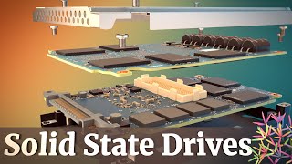
00:00 - Exploring CPUs, GPUs, DRAM, SSDs, and SOCs
01:07 - Introduction to the Photolithography Systems
04:11 - Printing Nanoscopic Lines
06:09 - The Basics of CPU Manufacturing
10:50 - Different Types of Lithography Tools EUV vs DUV
12:51 - Why we use Extreme Ultra Violet Light
15:31 - Producing the EUV Light using Tin Droplets
18:21 - The Illumination Optics
19:09 - The Incredible Engineering inside EUV Lithography
19:49 - Bragg Reflections
20:54 - Illumination Settings
22:30 - ASML Sponsorship
22:58 - Exploring the Photomask or Reticle
25:05 - Chip Patterns on a 300mm Wafer
27:27 - Branch Education Hours of Work
28:19 - Projection Optics Rayleigh's Criterion Equation
30:53 - Lithography Cluster
32:27 - Wafer Alignment
35:07 - Photoresist
36:01 - Wafer Transport
37:52 - Outro
Lead Animator: Mike Radjabov
Animation Team: Sherdil Davronov, Adrei Dulay, Muazzam Azizova, Abdulaziz Zokirov
Research, Script and Editing: Teddy Tablante
Twitter: @teddytablante
Modeling: Prakash Kakadiya
Image Editing: Randy Catequista
Voice Over: Phil Lee
Sound Design by Drilu: www.drilu.world
Sound Design and mix: David Pinete
Additional Sound Design: Raúl Núñez
Supervising Sound Editor: Luis Huesca
Erratum:
Wikipedia contributors. "Extreme Ultraviolet Lithography", "Photolithography". Wikipedia, The Free Encyclopedia. Wikipedia, The Free Encyclopedia, Visited May 19th 2025
A lot of information was gotten from the Semislides YouTube Channel. Additional input was provided by ASML
#EUV #Chips #ASML